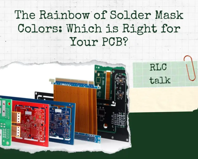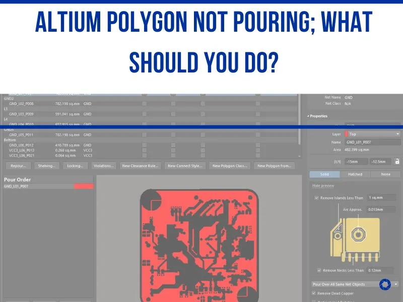
Altium Polygon Not Pouring; What Should You Do?
A group design object called a polygon pour is constructed from more basic primitive objects. Using Region objects or a fusion of Track and Arc objects, polygon pours are used to create a solid or hatched (lattice) area on a PCB layer.
But what can you do when the Altium polygon is not pouring? That is what we’re going to discuss in this article. So stick around until the end to find out what you’ve been looking for.
What is polygon in PCB?
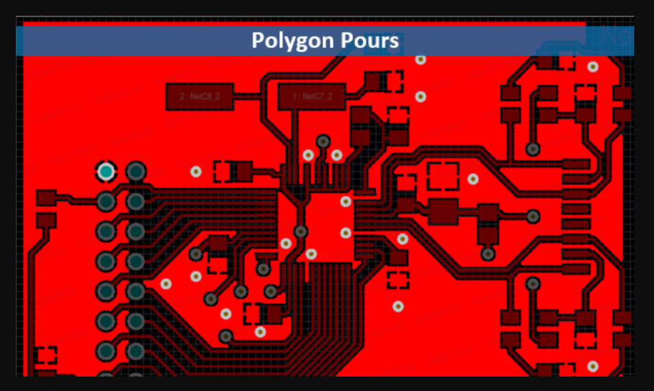
Polygons are regions of the PCB that are filled or flooded with copper and are also referred to as copper pours or polygon pours.
This area is filled with copper and has a predetermined clearance after being poured around the existing components and traces.
What really is polygon Pouring in Altium?
A polygon pour is a group design object, meaning it is composed of arcs, regions, and other simpler primitive objects. A solid polygon pour can be used to designate a ground-connected area for electromagnetic shielding or an area for carrying large power supply currents on a signal layer.
On the other hand, Polygon Pouring in Altium is a feature that allows you to quickly fill an entire area on a printed circuit board (PCB) with a solid copper region. This is useful for creating ground planes and other large areas of copper on a PCB. By pouring a large copper area, you can reduce the amount of time spent manually routing copper traces and can also reduce the overall complexity of a design.
How to pour polygon in Altium?
Here is how to use a polygon port in the Altium step by step.
- Select “Polygon Pour” from the “Place” menu in the top toolbar.
- Choose the layer on which you want to place the polygon.
- Click on the “Create Polygon” button in the Polygon Pour dialog box.
- Click on the board to place the first corner of the polygon.
- Continue to click on the board to place the other corners of the polygon.
- When you have finished adding corners, double click on the first corner to close the polygon.
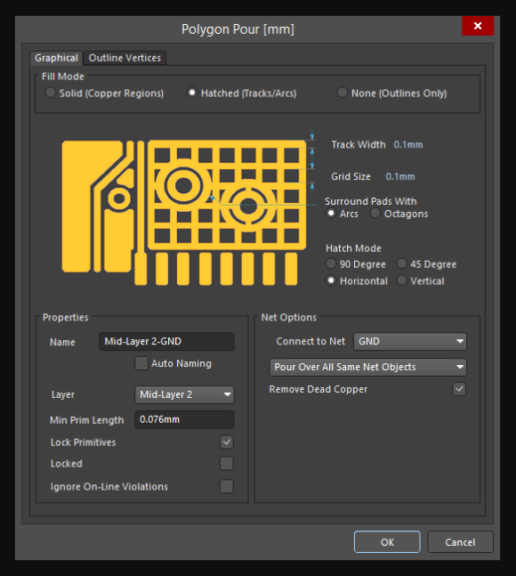
- Select the “Properties” tab in the Polygon Pour dialog box.
- Choose the fill type, such as solid or hatch.
- Select the “Rules” tab in the Polygon Pour dialog box.
- Set the layer, grid size, and other parameters to set the rules for the polygon pour.
- Click “OK” to complete the polygon pour.
How do you shelve polygons in Altium?
In Altium, polygons are shelved by assigning them to a specific layer and adjusting the Polygon Pour Properties. To do this, select the polygon, right click, and select ‘Polygon Pour Properties’. From here, you can select the layer you wish the polygon to reside on.
How do you reduce a polygon point?
To reduce a polygon point, first select the polygon you want to edit. Then, use the reduce vertices tool (found in the edit menu) to reduce the number of points in the polygon. You can specify a tolerance level to determine how much the points should be reduced by.
Altium Polygon Not Pouring; What Should You Do?
If your Altium Polygon is not pouring, there are several steps you can take to troubleshoot and resolve the issue.
- Check the Polygon’s Net Name: Make sure that the Polygon’s Net Name matches the net name of the other components connected to it. This can be done in the Polygon Properties window.
- Check the Polygon’s Properties: Make sure that the Polygon’s Properties are set correctly. These can be accessed through the Polygon Properties window.
- Check the Polygon’s Size: Make sure that the Polygon’s size is not too small for the size of the board. If the Polygon is too small, it may not pour correctly.
- Check the Polygon’s Location: Make sure that the Polygon is located in the correct layer. If the Polygon is located in the wrong layer, it may not pour correctly.
- Check the Copper Pour Settings: Make sure that the Copper Pour Settings are set correctly for the board. These can be accessed through the Copper Pour dialog box.
- Check the Solder Mask Settings: Make sure that the Solder Mask Settings are set correctly for the board. These can be accessed through the Solder Mask dialog box.
- Check the Polygon’s Track Width: Make sure that the Polygon’s Track Width is set correctly for the board. This can be accessed through the Polygon Properties window.
If none of these steps resolve the issue, it may be necessary to contact Altium support for further assistance.
Altium polygon pour not filling: what can I do?
- Use a larger drill size for the vias. If you are using a small drill size, the vias will not be able to fill with the polygon pour.
- Increase the clearance between the vias and the polygon pour. If the clearance is too small, the polygon pour will not be able to properly fill the vias.
- Check the width of the outline of the polygon pour. If the outline is too narrow, the polygon pour may not be able to properly fill the vias.
- Make sure the design rules are set correctly. If the design rules are not set correctly, the polygon pour may not be able to fill properly.
If all else fails, try using a thermal relief option for the vias. This will allow the polygon pour to fill more easily.
How to Troubleshoot Component Placement Issues in Altium?
RLC talk
How to remove polygon pour in Altium?
To remove a polygon pour in Altium, right-click on the polygon pour and select the “Remove Polygon Pour” option from the menu.
This will delete the polygon pour and all associated data. Alternatively, you can select the polygon pour and press the delete key on your keyboard.
Altium polygon pour clearance; what should I know about that?
When creating a PCB in Altium, you can use polygons to define a clearance area around a component or trace. Polygons are a type of shape that are composed of multiple straight lines.
These lines can be used to create a custom clearance area that is specific to the item or trace that needs to be isolated. This can be useful for components that require a specific clearance area or for traces that must be isolated from other traces.
When creating a polygon for clearance, you should make sure that the lines are drawn in a way that will not interfere with other objects on the board.
Additionally, you should ensure that the lines are drawn in a way that meets the necessary clearance requirements.
Eagle vs Altium Designer PCB Software; Best Comparison.
rlc talk