Minimum Solder Mask Sliver – Ultimate Guide
To ensure your circuit boards function correctly, it is essential to have a good solder mask. This will protect the copper traces from being damaged by the molten solder. In addition, a good solder mask will also help keep your board looking nice and tidy.
Here are some tips on how to achieve the best results with your solder mask:
1. Make sure that your design is correct before you start soldering. This will minimize the chances of mistakes being made, which could damage the solder mask.
2. Use a minimal amount of solder when assembling your circuit boards. Excess solder can cause damage to the solder mask and may even prevent it from adhering correctly to the board surface.
3. Take care when positioning components on the board. If they are not placed correctly, they may interfere with the soldering process and cause damage to the solder mask.
4. Always use flux when soldering, especially with delicate pitch components. The change will help keep the solder in place and reduce the chances of it flowing under or around the component leads.”
Let’s explore what solder mask silver is and the minimum solder mask silver measurement you can use for any PCB project.
What Is A Solder Mask Sliver?
Solder mask sliver is an essential feature of PCB board design that helps to protect solder joints and ensure reliable electrical performance. It refers to the narrow gap of the solder mask between two solder pads on the same side of the board, creating a second barrier around solder joints.
This additional insulation helps to prevent solder shorts and electrical leakage, which is essential as boards become more densely packed with components. The solder mask sliver also protects solder joints from oxidation caused by exposure to air, adding an extra layer of shielding for boards operating in harsh conditions.
During manufacturing, a solder mask is typically applied after the soldering process but before other SMT components are placed on the board. Therefore, ensuring solder mask slivers are correctly set and inspected during the assembly process can help to guarantee maximum reliability from your PCBs.
In summary, solder mask sliver technology is an essential aspect of PCB design that helps designers create high-quality products with optimal yields and extended lifespans. Furthermore, ensuring sufficient solder mask slivers are included in plans will provide reliable performance across various applications.
Minimum Solder Mask Sliver Pcbway
On top of offering panels coated with the trusted ENIG finish, Pcbway also offers exceptional minimum solder mask sliver tolerances down to 100μm (green) or 150μm (other colors). This ensures excellent connection accuracy between components while providing optimal protection from oxidation and corrosion.
Minimum Solder Mask Sliver JLCPCB
JLCPCB recommended minimum spacing is 0.2 mm (8mils), meaning there should be at least a 0.05 mm “growth/mask opening” around the pad on each side to allow for any misregistration that could occur in production.
By following this recommendation, JLCPCB can ensure that your printed circuit board will have all components attached adequately with no unwanted connections due to excessive solder bridging irregularities or unintended shorts caused by incorrect amounts of solder residue on unexpected copper surfaces during PCB assembly processes.
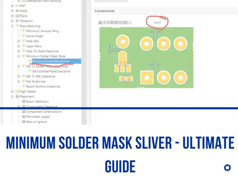
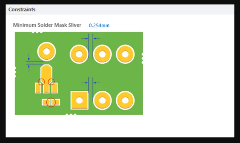
Minimum Solder Mask Sliver Altium
While it’s always essential to consider any dimensional tolerances when designing a board, the standard for minimum solder mask sliver Altium is 0.1 mm.
This requirement ensures that there will be enough solder mask coverage during the manufacturing process. In addition, some PCB assembly services may incorporate standards to meet specific design specifications. For example, PCB-POOL orders require an applied solder pad that is increased by 0.075 mm around the copper pad to guarantee a higher degree of accuracy.
rlc talk
What is solder mask clearance?
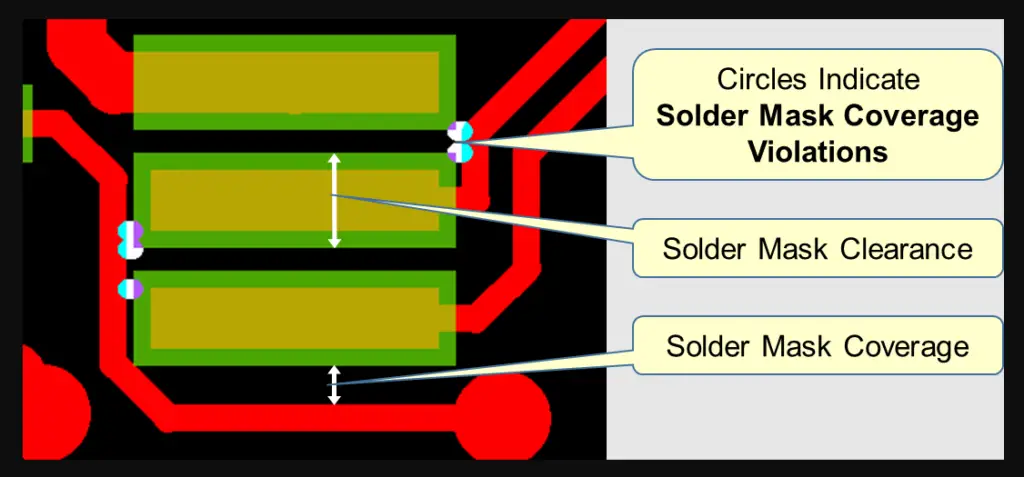
Solder mask clearance is a tolerance that determines how close the solder mask can be to the surface features of a PCB. The primary purpose of the solder mask is to protect the copper traces from being shorted by solder during the soldering process.
The ideal distance between the features and the solder mask is known as half pitch. However, due to manufacturing constraints, achieving a half angle is not always possible, so there needs to be a tolerance around this value.
How to Fix a Minimum Solder Mask Sliver Error
You’ve been working on your PCB design for hours and are ready to send it off to manufacturing. But then, disaster strikes! You notice a tiny sliver of solder mask during the final check between two pads. What does this mean? And more importantly, how do you fix it?
What Is a Minimum Solder Mask Sliver Error?
A minimum solder mask sliver error is a design error that can occur during the PCB manufacturing process. This error is typically caused by an incorrect Gerber file, which can cause the solder mask layer to be too thin in some regions of the PCB. As a result, exposed copper can lead to shorts or other issues during assembly.
Solving Minimum Solder Mask Sliver Error
You can fix a minimum solder mask sliver error in a few different ways. The first option is to increase the width of the exposed copper trace. This can be done by adding copper to the trace or by increasing the width of the trace itself.
Another option is to increase the size of the solder mask opening. This will ensure that there is sufficient coverage over the exposed copper trace. Finally, you can also use thermal relief pads to improve solder mask coverage in high-density areas.
There is another option…
- Open the Gerber file in a text editor. The file will be in the .drd or .dri format.
- Locate the line that contains the minimum solder mask sliver error. It will look something like this: %LPD*%
- Change the value on this line from 0.0010 to 0.0015.
- Save and close the file.
Remember, it’s always best to consult with a professional engineer or fabricator if you’re ever unsure about your PCB design. They’ll be able to help you troubleshoot any issues and get your design ready for manufacturing.
Eagle vs Altium Designer PCB Software; Best Comparison.
rlc talk